
MIRTEK AOI MV9 Series
- Home
- MIRTEK AOI MV9 Series
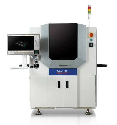
MIRTEC MV-9 Series – Advanced Full 3D Automated Optical Inspection System
The MIRTEC MV-9 Series is a premium inline 3D Automated Optical Inspection (AOI) system designed to deliver high-speed, high-precision PCB inspection. Equipped with a 25-megapixel high-resolution camera, four-direction QHD Moiré projection technology, and an 8-phase colour lighting system, it captures detailed 3D images for accurate defect detection. Its advanced vision technology supports inspection of miniature components, including 0201 mm chips.
Featuring a precision linear motor drive system, 10-megapixel digital side-view cameras, and MIRTEC’s OMNI-VISION® 3D/2D inspection technology, the MV-9 Series provides comprehensive inspection from multiple angles. Its advanced measurement capabilities help identify component placement issues, lifted leads, solder defects, tombstoning, and other PCB assembly problems, while the built-in SPC and repair software support effective quality monitoring and production control.
Technical Specifications
Advanced 3D and 2D inspection technology for precise PCB defect detection and production quality control.
| Technical Parameters | MV-9 | MV-9U | MV-9DL |
|---|---|---|---|
| PCB Specifications | |||
| Maximum PCB Size Range | 50 × 50 – 510 × 460 mm | 60 × 60 – 660 × 610 mm | 50 × 50 – 330 × 250 mm |
| Inspection Technology | |||
| 3D Inspection Technology | Digital Multi-Frequency Quad Moiré Technology | ||
| 2D Inspection Technology | ISIS® Vision System | ||
| Height Accuracy | ±3 μm | ||
| Maximum Component Height |
25MP Camera: 4 mm (7.7 μm option) 15MP Camera: 5 mm (15 μm option), 4 mm (10 μm option) |
||
| Inspection Items – 2D | Missing Component, Misalignment, Polarity, Tombstone, Manhattan, Bridge, Turn Over, Wrong Component, Scratch, Solder Ball, Foreign Body, Shift, Tilt, BGA Ball and Wave Solder Defects | ||
| Inspection Items – 3D | Missing Component, Height, Position, Lifted Package, Lifted Chip, Lifted Lead, Solder Fillet, Excessive Solder, Insufficient Solder, Open Solder, Double Chip, Manhattan, Tombstone, Tilt, Dimension and Foreign Objects | ||
| Vision System | |||
| Top Camera | 25 Mega Pixel (15 Mega Pixel Optional) | ||
| 25MP Camera Resolution | 7.7 μm | ||
| 15MP Camera Resolution | 15 μm / 10 μm Options | ||
| Lens Configuration | Precision Telecentric Compound Lens | ||
| Lighting System | Eight Phase Colour Lighting | ||
| Side Viewer® Camera System | 10 Mega Pixel Digital Colour Side Cameras (4 Cameras) | ||
| 25MP Camera FOV |
CXP: 39.42 × 39.42 mm Camera Link: 38.93 × 38.93 mm |
||
| 15MP Camera FOV |
15 μm: 58.56 × 58.56 mm 10 μm: 39.04 × 39.04 mm |
||
| Inspection Performance | |||
| 2D Inspection Speed – 25MP |
CoaXPress: 72 fps Camera Link: 23 fps |
||
| 2D Inspection Speed – 15MP |
CoaXPress: 120 fps Camera Link: 37 fps |
||
| 3D / 2D Inspection Speed – 25MP |
CoaXPress: 72 fps Camera Link: 23 fps |
||
| 3D / 2D Inspection Speed – 15MP |
CoaXPress: 120 fps Camera Link: 37 fps |
||
| System Specifications | |||
| PCB Top Side Clearance | 45 mm | ||
| PCB Bottom Side Clearance | 25 mm (50.8 mm Optional) | ||
| Maximum PCB Warpage | ±3 μm | ||
| Barcode System (1D / 2D) | Keyence, Leuze, Data Logic, Cognex and Micro Scan | ||
| Built-in SPC | Statistical Process Control Software | ||
| Built-in Repair | Repair Software | ||
| OLTT | Off-Line Teaching Tool Software (Optional) | ||
| Minimum Measurement Size |
25MP (7.7 μm): 0201 Chip / 0.3 Pitch 15MP (15 μm): 0603 Chip / 0201 Chip (inch) / 0.4 Pitch 15MP (10 μm): 03015 Chip / 0.3 Pitch |
||
| Motion & Positioning System | |||
| Robot Positioning System | Precision Linear Drive Motor System (X/Y Axis) | ||
| Positioning Resolution | 0.5 μm | ||
| Positioning Repeatability | ±2 μm | ||
| Power & Utility Requirements | |||
| Power Supply | Single Phase, 200–240V, 50–60Hz, 1.1 kW | Refer to model-specific configuration | Single Phase, 200–240V, 50–60Hz, 1.5 kW |
| Air Supply | 5 kgf/cm² (0.5 MPa) | ||
| Dimensions & Weight | |||
| Machine Dimensions (W × D × H) | 1,250 × 1,500 × 1,600 mm | 1,400 × 1,650 × 1,600 mm | 1,250 × 1,500 × 1,600 mm |
| Machine Weight | Approx. 1,200 kg | Approx. 1,500 kg | Approx. 1,400 kg |
Key Features
Innovative vision and measurement technologies for precise inspection and dependable PCB production quality.
25MP High-Resolution Camera
Captures highly detailed PCB images with 7.7 μm resolution, supporting precise inspection of miniature components and fine-pitch assemblies.
4-Way Multi-Frequency Moiré Technology
Uses four-direction 3D projection with high- and low-frequency patterns to capture component height information while reducing inspection blind spots.
QHD Projection Technology
Fine fringe pattern projection improves height-change detection, chip measurement repeatability and solder fillet inspection accuracy.
8-Phase Colour Lighting System
Combines eight lighting conditions to produce clear, low-noise images for accurate component, lifted-lead and solder joint inspection.
10MP Side Viewer® System
Four high-resolution side cameras provide multi-directional component inspection and convenient visual verification of potential defects.
Precision Linear Motor System
Provides 0.5 μm positioning resolution and ±2 μm repeatability for stable, accurate and consistent inspection movement.
Intellisys® System
Supports remote monitoring, SPC analysis, debugging and repair functions to help manage inspection issues and reduce production losses.
Comprehensive 3D & 2D Inspection
Identifies missing components, misalignment, tombstoning, lifted leads, solder bridges, insufficient solder and other PCB assembly defects.
Industries we serve
Our Automated Optical Inspection (AOI) solutions support a wide range of electronics manufacturing industries by delivering intelligent defect detection, enhanced quality assurance, and reliable inspection throughout the SMT production process.