3D X-Ray Inspection System S8800
- Home
- 3D X-Ray Inspection System S8800
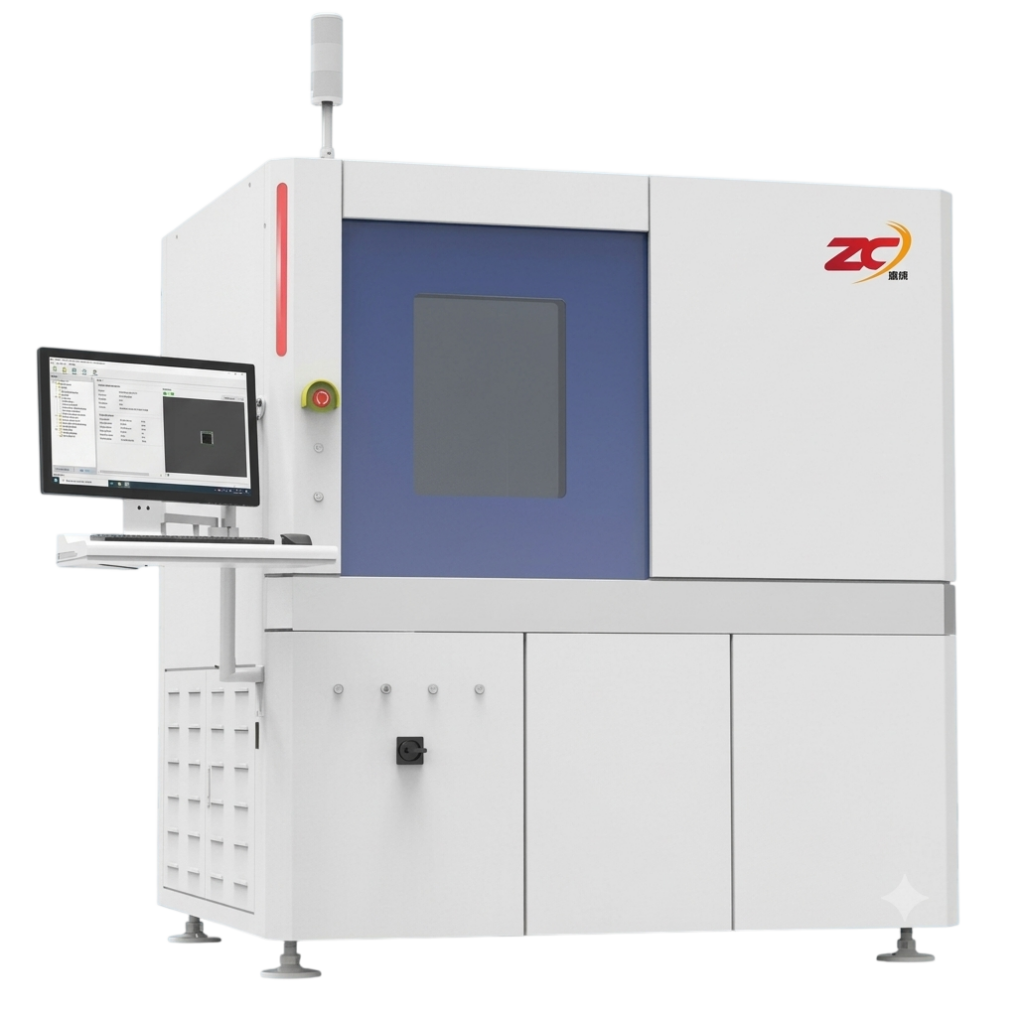
S8800 High-Resolution 3D X-Ray Inspection System with Multi-Mode CT
The S8800 is a versatile 3D X-ray inspection system integrating 2D/3D scanning and multiple CT modes (Planar CT, Axial CT) for high-precision defect detection in PCB, SMT, IGBT, wafer packaging, and discrete components. Equipped with a 130kV micro-focus X-ray source (3.0µm resolution) and advanced reconstruction algorithms, it delivers ultra-clear imaging for voids, cracks, solder joint defects, and internal structure analysis. With a large sample capacity (up to 1000×650mm) and Industry 4.0 compatibility, it supports both lab and production line applications.
The system features proprietary self-developed CT reconstruction technology and AI-enhanced image processing to significantly boost micro-details visibility, such as defects smaller than 3µm in solder joints. It also incorporates multi-layer noise reduction, real-time edge enhancement, and CCD optical navigation for rapid sample positioning, ensuring seamless enterprise integration with MES/ERP systems.
S8800 High-Resolution 3D X-Ray Inspection Machine Technical Specifications
Comparative technical specifications of the S8800 system across V1 and V2 models.
| Specification / Parameter | Model V1 | Model V2 |
|---|---|---|
| Manufacturer | WISDOMSHOW | |
| Country of Origin | China | |
| X-Ray Source Type | Closed micro-focus tube | |
| X-Ray Voltage | 130 kV | |
| Resolution | 3.0 μm | |
| Detector Type | High-performance flat panel | |
| Scanning Modes | 2D X-ray, Circular Planar CT, Axial CT (optional) | 2D X-ray, Linear Planar CT, Axial CT (optional) |
| Max Sample Size | 800 × 580 mm | 1000 × 650 mm |
| Scan Range | 2D: 510 × 510 mm; Planar CT: Φ420 mm | 1000 × 650 mm |
| Tilt Angle | ±70° | ±50° |
| Equipment Dimensions | 1843 × 1670 × 2104 mm | 2974 × 2167 × 2091 mm |
| Machine Weight | 3500 kg | 7000 kg |
| Power Supply | AC 220V, 3KVA | AC 220V, 6KVA |
| Radiation Safety | Less than 1 μSv/h | |
Advanced Features of the S8800 3D X-Ray Inspection System
Multi-mode CT scanning, ultra-high resolution, and smart factory integration.
Multi-Mode CT Scanning
Supports Planar CT for large flat samples like PCBs and SMT, and Axial CT for high-precision 3D imaging of small components like IGBTs and wafer bumps.
Advanced Imaging Algorithms
Equipped with proprietary self-developed CT reconstruction technology, AI-enhanced image processing, multi-layer noise reduction, and real-time edge enhancement.
Ultra-High Resolution
Features a 130kV micro-focus X-ray source with 3.0µm spatial resolution for clear visualization of solder voids, cracks, and TSV defects.
Large Sample Capacity
Accommodates large-scale testing requirements with sample capacities up to 1000 × 650 mm (V2 model).
CCD Optical Navigation
Provides rapid and precise sample positioning through built-in CCD optical navigation systems.
Industry 4.0 Ready
Seamlessly integrates with MES and ERP systems for automated smart factory reporting and traceability.
Industries we serve
Our Automated Optical Inspection (AOI) solutions support a wide range of electronics manufacturing industries by delivering intelligent defect detection, enhanced quality assurance, and reliable inspection throughout the SMT production process.